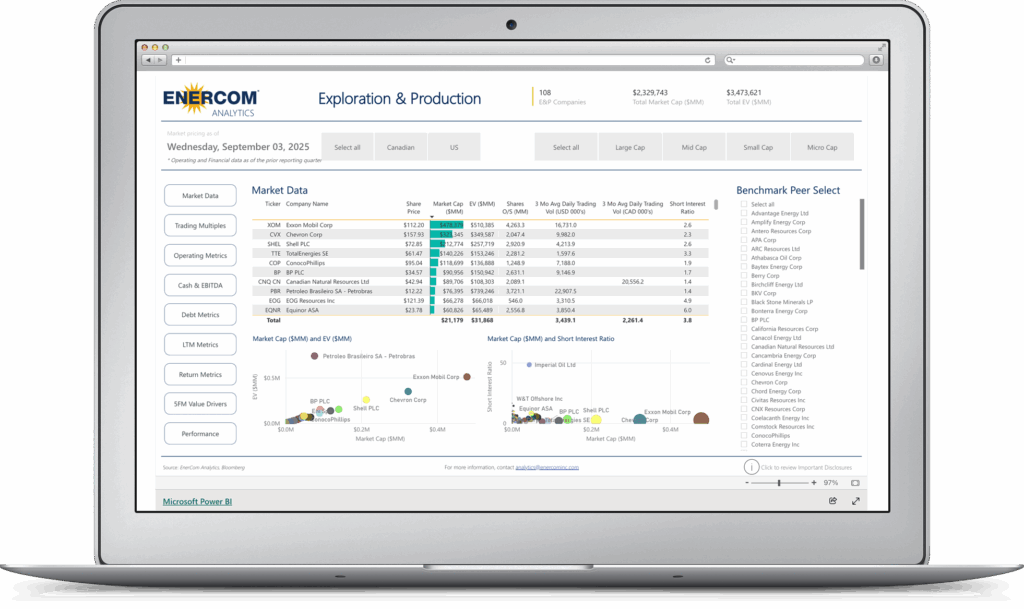
March 17, 2016 - 9:05 PM EDT
Print Email Article Font Down Font Up
Researchers Submit Patent Application, "Nitride Semiconductor Quantum Cascade Laser", for Approval (USPTO 20160064901)

By a News Reporter-Staff News Editor at Electronics Newsweekly -- From

Washington, D.C.
, VerticalNews journalists report that a patent application by the inventors TERASHIMA, Wataru (Wako-shi, JP); HIRAYAMA, Hideki (Wako-shi, JP), filed on August 11, 2015, was made available online on March 10, 2016.

No assignee for this patent application has been made.

News editors obtained the following quote from the background information supplied by the inventors: "The present disclosure relates to a semiconductor quantum cascade lasers. More specifically, the present disclosure relates to a nitride semiconductor quantum cascade laser that includes a gallium nitride based material.

"Recently, for solid-state lasers operating in wavelength ranges in which electromagnetic wave radiation by inter-band transition is difficult, quantum cascade lasers (QCLs) that utilize inter-subsub band transition of conduction carriers without jumping across a band gap are regarded as promising. QCLs are expected to be put into practical use due to their properties, such as ultra-compactness, high efficiency/high output power, narrow linewidth, long life, continuous wave operation, inexpensiveness, and high durability; and the development of QCLs has been in progress for mid-infrared and terahertz frequency ranges. In particular, when terahertz quantum cascade lasers (THz-QCLs) capable of lasing in a terahertz frequency range of 0.1 THz to 30 THz are realized, the THz-QCLs are expected to be applied to such fields as medical imaging, security check, and high-speed wireless communication. However, lasing operation of THz-QCLs has only been reported in a frequency range of 1.2 to 5.2 THz or a range over 12 THz. That is, lasing operations in a frequency range close to 1 THz, or in a frequency range between 5.2 THz and 12 THz has never been reported. It is an important issue to realize a THz-QCL capable of lasing in such frequency ranges, or in the unexplored frequency ranges.

"For conventional materials of THz-QCLs, GaAs-, InP-, and InSb-based semiconductors have been employed. However, even when these materials are employed, it is difficult to realize a THz-QCL of frequency range of 5 to 12 THz. This is because, energy bands of scattering through Froehlich interaction between electrons and longitudinal-optical (LO) phonons for these materials have an overlap with a frequency range of 5 to 12 THz. For example, the LO-phonon energy E.sub.LO for GaAs is 36 meV, which is equivalent to 9 THz. In addition, population inversion is degraded due to the fact that refilling lower lasing level with electrons, called thermal backfilling, is likely to occur with GaAs-, InP-, and InSb-based semiconductors, which is also disadvantageous to lasing operation.

"It is expected that employing a nitride semiconductor, in place of the above-mentioned conventional materials such as GaAs, allows a THz-QCL of a frequency range of 5 to 12 THz to be realized. With a GaN-based material, which is a typical one of the nitride semiconductors, the LO-phonon energy E.sub.LO is 90 meV, namely, about three times higher than that of GaAs. Because of the high LO-phonon energy, the phonon domain shifts to near 22 THz, which is equivalent to the energy of the LO-phonon, enabling the prevention of absorption due to electron-LO-phonon scattering in a frequency range of 5 to 12 THz. Furthermore, a higher energy of electron-LO-phonon scattering is advantageous also in that operation at high temperature can be expected.

"It is noted that a theoretical calculation result is disclosed in the case that a super lattice having two well layers of GaN and two barrier layers of AlGaN in each unit corresponding to one period is adopted (see for example, Patent Literature 1, claim 2 therein). However, when a crystal lattice is grown on a polarized surface, which is important in terms of crystal growth, it is shown that a gain takes on negative values at energies corresponding to frequencies of 5 THz or above, or about 20 meV or more. Therefore, lasing operation at frequencies over 5 THz cannot be expected (see for example, Patent Literature 1, FIG. 17). In addition, in this disclosure, actual operation is not predicted specifically. For example, lasing frequencies to be operated are not identified."

As a supplement to the background information on this patent application, VerticalNews correspondents also obtained the inventors' summary information for this patent application: "The present inventorshave attempted, from both of theoretical and experimental perspectives, demonstration of a THz-QCL for which a nitride semiconductor material is employed. One of the objects is to fabricate a THz-QCL that performs lasing operation at any one of frequencies ranging from 5 to 12 THz, which is one of the above-mentioned unexplored frequency ranges. The present inventorshave fabricated a structure having four well layers per unit using a GaN-based material ('a four quantum well structure', see Non Patent Literature 1), and furthermore have confirmed that light emission, or radiation, took place due to inter-subsub band transition in such a THz-QCL employing a GaN-based material to which the four quantum well structure is fabricated (Non Patent Literature 2).

"However, a THz-QCL has not been necessarily realized as intended (see Non Patent Literature 1 and Non Patent Literature 3). First, the radiation was obtained for 1.4 to 2.8 THz, rather than for a frequency of 7.6 THz which was target one by design. Second, the observed light emission was not of stimulated emission operation in a reproducible manner (lasing operation of the laser); rather what was observed was merely a spontaneous emission operation.

"In order to solve the above problems, the present inventorsconducted detailed analysis of actual operation for the THz-QCL with a GaN-based material adopting the four quantum well structure by comparing the operation with one in theoretical calculation. The analysis showed that the radiation at the above unexpected frequencies resulted from spontaneous emission of transition between a pair of levels whose energy values were expected to be degenerated. It was confirmed that the pair of levels in the actual crystal lattice were in non-degenerate states, or their degeneracy was lifted, and the radiation occurred at a frequency corresponding to a resulted slight energy difference.

"The present disclosure has an object to solve at least one of the above-mentioned problems. That is, the present disclosure is to provide a THz-QCL that performs lasing operation in the unexplored frequency range, thereby contributing to the expansion of the frequency range of THz-QCLs.

"Based on the above-mentioned analysis, the present inventors have envisioned that the unintended radiation in a four quantum well structure should be originated from a complex configuration itself, in which a variety of well layers are contained in a single unit structure, in the case where the four quantum well structure is formed on a polarized plane of a substrate. In addition, the inventors have paid attention to each level of a pair of levels that provokes spontaneous emission. Then, based on the specific structure of the pair of levels that actually contributes to the above spontaneous emission, we have attempted to design a new sub band structure. Moreover, we have fabricated a THz-QCL having such a structure, and have confirmed that lasing operation has been actually realized.

"That is, in one aspect of the present disclosure, there is provided a quantum cascade laser element including a super lattice formed by a crystal of a nitride semiconductor, wherein the super lattice includes a plurality of unit structures, wherein each unit structure is formed to include a first barrier layer, a first well layer, a second barrier layer, and a second well layer disposed in this order, by repeatedly stacking a barrier layer and a well layer respectively having high and low potentials with respect to conduction-band electrons, wherein, in each unit structure, an energy level structure for electrons under a bias electric field in a stacking direction due to external voltage has: a mediation level that has a significant probability of finding an electron in at least one of the first well layer and the second well layer; an upper lasing level that has a significant probability of finding an electron in the first well layer; and a lower lasing level that has a significant probability of finding an electron in the second well layer, wherein under the bias electric field, an energy value of the mediation level is close to an energy value of one of levels, out of an upper lasing level and a lower lasing level each belonging to any one of the unit structure and another unit structure adjacent thereto, and is separated from an energy value of the other level by at least an energy value of a longitudinal-optical (LO) phonon of the crystal of the nitride semiconductor making the super lattice, and wherein the energy value of the LO-phonon of the nitride semiconductor making the super lattice is greater than a photon energy for an electromagnetic wave to be emitted by stimulated emission from an electron that makes a transition from the upper lasing level to the lower lasing level under the bias electric field.

"Additionally, we have found that adopting an additional level may facilitate lasing operation between levels in the above-mentioned sub band structure.

"That is, in another aspect of the present disclosure, there is provided a quantum cascade laser element including a super lattice formed by a crystal of a nitride semiconductor, wherein the super lattice includes a plurality of unit structures, wherein each unit structure is formed to include a first barrier layer, a first well layer, a second barrier layer, a second well layer, a third barrier layer, and a third well layer disposed in this order, by repeatedly stacking a barrier layer and a well layer respectively having high and low potentials with respect to conduction-band electrons, wherein, in each unit structure, an energy level structure for electrons under a bias electric field in a stacking direction due to external voltage has: a transport level that has a significant probability of finding an electron in the first well layer; an upper lasing level that has a significant probability of finding an electron existence in the second well layer, the upper lasing level having an energy value lower than the transport level by at least an energy value of a longitudinal-optical (LO) phonon of the crystal of the nitride semiconductor making the super lattice; a lower lasing level that has a significant probability of finding an electron in the third well layer; and a depopulation level that has a significant probability of finding an electron in the third well layer, the depopulation level having an energy value lower than an energy value of the lower lasing level by at least an energy value of the LO-phonon, wherein the energy value of the LO-phonon of the nitride semiconductor making the super lattice is greater than a photon energy for an electromagnetic wave.

"Furthermore, in another aspect of the present disclosure, there is provided a quantum cascade laser element including a super lattice formed by a crystal of a nitride semiconductor, wherein the super lattice includes a plurality of unit structures, each unit structure is formed to include a first barrier layer, a first well layer, a second barrier layer, a second well layer, a third barrier layer, and a third well layer disposed in this order by repeatedly stacking a barrier layer and a well layer respectively having high and low potentials with respect to conduction-band electrons, wherein, in each unit structure, an energy level structure for electrons under a bias electric field in a stacking direction due to external voltage has: a transport level that has a significant probability of finding an electron in the first well layer; an injection level that has a significant probability of finding an electron in the second well layer; an upper lasing level that has a significant probability of finding an electron in the second well layer, the upper lasing level having an energy value lower than the injection level by at least an energy value of a longitudinal-optical (LO) phonon that is exhibited by the crystal of the nitride semiconductor making the super lattice; a lower lasing level a significant probability of finding an electron in the third well layer; and a depopulation level that has a significant probability of finding an electron in the third well layer, the depopulation level having an energy value lower than the lower lasing level by at least an energy value of the LO-phonon, wherein the energy value of the LO-phonon of the nitride semiconductor making the super lattice is greater than the photon energy for an electromagnetic wave.

"In the present application, an electromagnetic wave in a THz range may refer to an electromagnetic wave in a frequency range of about 0.1 THz to 30 THz, namely, in a wavelength range of about 10 .mu.m to 3 mm. In addition, the unexplored frequency range may be a frequency range of electromagnetic wave of over 5.2 THz and 12 THz or under. The unexplored frequency range may be often roughly described herein as 5 to 12 THz. Furthermore, element structures or functions in the present application may be described by using technical terms converted or borrowed from those technological fields of electronic devices and physics that are related to visible lights or infrared rays. For this reason, even when electromagnetic waves at a frequency or wavelength range far different from those for the visible light are concerned, such terms as 'laser', 'light emission', or such prefixes as 'optical-' or 'photo-' may be adopted.

"In one aspect of the present disclosure, a quantum cascade laser element that radiates electromagnetic waves at 5 to 12 THz is provided.

BRIEF DESCRIPTION OF THE SEVERAL VIEWS OF THE DRAWINGS

"In the drawings, identical reference numbers identify similar elements or acts. The sizes and relative positions of elements in the drawings are not necessarily drawn to scale.

"FIG. 1 is a graph showing lasing operations of various conventional THz-QCLs, as a function of lasing frequency and operation temperature.

"FIG. 2A is a schematic diagram of electron energy illustrating a phenomenon relevant to temperature that has an influence on operation temperature and lasing frequencies in a THz-QCL, in real space along a stacking direction.

"FIG. 2B is a schematic diagram of electron energy illustrating a phenomenon relevant to temperature that has an influence on operation temperature and lasing frequencies in a THz-QCL, in an in-plane wave number space.

"FIG. 3 is a perspective view showing the schematic structure of a conventional THz-QCL and a THz-QCL in an embodiment of the present disclosure.

"FIG. 4 is a graph of positional dependence of electric potential in a THz-QCL having a conventional four quantum well structure, and the electron probability distribution calculated from the wave function of each sub band.

"FIG. 5A is a graph showing positional dependence of electric potential, and an electron probability distribution calculated from the wave function of each sub band, in the configuration of a THz-QCL fabricated by an MBE in an embodiment of the present disclosure

"FIG. 5B is a schematic diagram of the behavior of an electron in a reduced depiction scheme.

"FIG. 6A is a graph depicting the energy difference between sub bands.

"FIG. 6B is a plot of dipole moment with respect to a bias electric field strength, in a THz-QCL fabricated by an MBE in an embodiment of the present disclosure.

"FIG. 7A is a graph depicting electric current-light intensity characteristics and electric current-voltage characteristics obtained through observation of a THz-QCL fabricated by an MBE in an embodiment of the present disclosure.

"FIG. 7B is a graph depicting emission spectra for several currents, obtained through observation of a THz-QCL fabricated by an MBE in an embodiment of the present disclosure.

"FIG. 8A is a graph showing positional dependence of electric potential and an electron probability distribution calculated from the wave function of each sub band, for a structure of the THz-QCL fabricated by an MOCVD in an embodiment of the present disclosure.

"FIG. 8B is a schematic diagram of behavior of an electron in a reduced depiction scheme for the embodiment shown in FIG. 8A.

"FIG. 9A is a graph depicting energy differences between sub bands with respect to a bias electric field strength, in a THz-QCL fabricated by an MOCVD in an embodiment of the present disclosure.

"FIG. 9B is a graph depicting energy differences between dipole moments with respect to a bias electric field strength, in a THz-QCL fabricated by an MOCVD in an embodiment of the present disclosure.

"FIG. 10A is a graph depicting electric current-light intensity characteristics and electric current-voltage characteristics obtained through observation of a THz-QCL fabricated by an MOCVD in an embodiment of the present disclosure.

"FIG. 10B is a graph depicting emission spectra for several currents obtained through observation of a THz-QCL fabricated by an MOCVD in an embodiment of the present disclosure.

"FIG. 11 is a graph as in FIG. 1, to which values obtained by demonstrating the THz-QCL in an embodiment are added.

"FIG. 12A is a TEM cross-section micrographs of super lattices grown by an MBE technique in an embodiment of the present disclosure.

"FIG. 12B is a TEM cross-section micrograph of super lattices grown by an MOCVD technique.

"FIG. 13A is a graph of predicted and measured X-ray diffraction intensity values for super lattices grown using an MBE technique in an embodiment of the present disclosure.

"FIG. 13B is a graph of predicted and measured X-ray diffraction intensity values for super lattices of the embodiment shown in FIG. 13A, grown by an MOCVD technique.

"FIG. 14A shows mapping images of X-ray diffraction into a reciprocal lattice space of super lattices that are grown using an MBE technique in an embodiment of the present disclosure

"FIG. 14B shows mapping images of X-ray diffraction into a reciprocal lattice space of super lattices according to the embodiment shown in FIG. 14A, grown using an MOCVD technique.

"FIG. 15A shows performance diagrams of the investigated results of lasing frequencies through theoretical calculation, with variations in composition ratio that has an influence on barrier height and variations in thickness of the well layer, which are design parameters of the THz-QCL in an embodiment of the present disclosure.

"FIG. 15B shows performance diagrams of the investigated results of lasing frequencies through theoretical calculation, with variations in bias electric field and variations in thickness of the well layer in an embodiment of the present disclosure.

"FIG. 16A is a graph showing positional dependence of electric potential and an electron probability distribution calculated from the wave function of each sub band, for structures of a THz-QCL for which a GaN/InGaN material is employed in a structure in which lasing occurs at around 6 THz, according to an embodiment of the present disclosure.

"FIG. 16B is a graph showing positional dependence of electric potential and an electron probability distribution calculated from the wave function of each sub band, for structures of a THz-QCL for which a GaN/InGaN material is employed in a structure in which lasing occurs at around 10 THz, according to an embodiment of the present disclosure. and for another structure with which lasing occurs at around 10 THz (FIG. 16B).

"FIG. 17 is graph of calculation result showing variations in lasing frequency as a function of In composition ratio, which has an influence on the barrier height of a THz-QCL for which a GaN/InGaN material is employed in an embodiment of the present disclosure.

"FIG. 18A is a graph showing positional dependence of electric potential and an electron probability distribution calculated from the wave function of each sub band, for structures of a THz-QCL for which a AlGaN/GaN material formed on a nonpolar plane of an AlN substrate is employed for one structure in which lasing occurs at around 10 THz, in an embodiment of the present disclosure.

"FIG. 18B is a graph showing positional dependence of electric potential and an electron probability distribution calculated from the wave function of each sub band, for structures of a THz-QCL for which a AlGaN/GaN material formed on a nonpolar plane of an AlN substrate is employed for one structure in which lasing occurs at around 7.3 THz, in an embodiment of the present disclosure.

"FIG. 19 is a graph of a calculation result showing variations in lasing frequency with respect to an Al composition ratio, which has an influence on the barrier height of the THz-QCL for which an AlGaN/GaN material formed on a nonpolar plane of an AlN substrate is employed in an embodiment of the present disclosure.

"FIG. 20A is a graph showing positional dependence of electric potential and electron probability distribution calculated from the wave function of each sub band, for structures of a THz-QCL for which a GaN/InGaN material formed on a nonpolar plane of a GaN substrate is employed in a structure in which lasing occurs at around 12 THz, in an embodiment of the present disclosure.

"FIG. 20B is a graph showing positional dependence of electric potential and electron probability distribution calculated from the wave function of each sub band, for structures of a THz-QCL for which a GaN/InGaN material formed on a nonpolar plane of a GaN substrate is employed in a structure in which lasing occurs at around 9 THz, in an embodiment of the present disclosure.

"FIG. 21 is a graph of a calculation result showing variations in lasing frequency with respect to an In composition ratio, which has an influence on the barrier height of the THz-QCL for which an GaN/InGaN material formed on a nonpolar plane of an GaN substrate is employed in an embodiment of the present disclosure.

"FIG. 22A is a graph of calculation result showing positional dependence of electric potential, and electron probability distribution calculated from the wave function of each sub band, in the configuration of a THz-QCL in an embodiment of the present disclosure with which lasing frequencies of 12 to 19.5 THz can be obtained.

"FIG. 22B is a schematic diagram of the behavior of an electron in a reduced depiction scheme, according to an embodiment of the present disclosure.

"FIG. 23A is a graph of calculation result showing variations in lasing frequencies with respect to composition ratio, which has an influence on barrier height, for a THz-QCL in an embodiment of the present disclosure with which lasing frequencies of 12 to 19.5 THz can be obtained. FIG. 23B is a graph of calculation result showing variations in lasing frequencies with respect to bias electric field, which has an influence on barrier height, for the THz-QCL of FIG. 23A.

"FIG. 24A is a graph showing positional dependence of electric potential and electron probability distribution calculated from the wave function of each sub band, for structures of a THz-QCL in an embodiment of the present disclosure with which lasing frequencies of 7 to 10.5 THz can be obtained.

"FIG. 24B is a schematic diagram of the behavior of an electron in a reduced depiction scheme according to the embodiment shown in FIG. 24A.

"FIG. 25A is a graph of a calculation result indicating variations in lasing frequency with respect to composition ratio that has an influence on barrier height for a THz-QCL in an embodiment of the present disclosure with which lasing frequencies of 7 to 10.5 THz can be obtained.

"FIG. 25B is a graph of a calculation result indicating variations in lasing frequency with respect to bias electric field that has an influence on barrier height for a THz-QCL according to the embodiment of FIG. 25A.

"FIG. 26A is a graph of a calculation result showing positional dependence of electric potential, and electron probability distribution calculated from the wave function of each sub band, for a structure of a THz-QCL in an embodiment of the present disclosure with which lasing frequencies near 6 THz can be obtained.

"FIG. 26B is a schematic diagram of the behavior of an electron in a reduced depiction scheme according to the embodiment of FIG. 26A.

"FIG. 27A is a graph of calculation result showing positional dependence of electric potential, and electron probability distribution calculated from the wave function of each sub band, for a structure of a THz-QCL in an embodiment of the present disclosure with which lasing frequencies near 6 THz can be obtained.

"FIG. 27B is a schematic diagram of the behavior of an electron in a reduced depiction scheme according to the embodiment of FIG. 27A.

"FIG. 28 is a graph of a calculation result on a structural example for lasing operation at a low frequency in a pure-three-level-system QCL in an embodiment of the present disclosure, showing positional dependence of electric potential, and an electron probability distribution calculated from the wave function of each sub band, for a structure of a THz-QCL with which lasing frequencies of 1.8 to 4.3 THz are obtained.

"FIG. 29A shows graphs of calculation results indicating variations in lasing frequency with respect to composition ratio that has an influence on barrier height for a THz-QCL with which lasing frequencies of 1.8 to 4.3 THz are obtained, for a structural example in which a pure-three-level-system QCL for lasing operation in a similar manner to that shown in FIG. 28.

"FIG. 29B shows graphs of calculation results indicating variations in lasing frequency with respect to bias electric field that has an influence on barrier height for a THz-QCL with which lasing frequencies of 1.8 to 4.3 THz are obtained, for a structural example in which a pure-three-level-system QCL for lasing operation in a similar manner to that shown in FIG. 28.

"FIG. 30 is a graph of the measured intensity values obtained by causing an output from the THz-QCL sample having the sub band structure of the THz-QCL shown in FIG. 5A to pass through a wire-grid polarizer.

"FIG. 31 is a graph showing electric current-light intensity characteristics and electric current-voltage characteristics observed with temperature varied using a THz-QCL sample having a sub band structure of the THz-QCL as shown in FIG. 5A.

"FIG. 32 is a graph of lasing thresholds J.sub.th as a function of temperature, obtained from the measured value in FIG. 31."

For additional information on this patent application, see: TERASHIMA, Wataru; HIRAYAMA, Hideki. Nitride Semiconductor Quantum Cascade Laser. Filed August 11, 2015 and posted March 10, 2016. Patent URL: http://appft.uspto.gov/netacgi/nph-Parser?Sect1=PTO2&Sect2=HITOFF&u=%2Fnetahtml%2FPTO%2Fsearch-adv.html&r=1594&p=32&f=G&l=50&d=PG01&S1=20160303.PD.&OS=PD/20160303&RS=PD/20160303

Keywords for this news article include: Patents, Electronics, Electromagnet, Semiconductor.

Our reports deliver fact-based news of research and discoveries from around the world. Copyright 2016, NewsRx LLC

DISCLOSURE: The views and opinions expressed in this article are those of the authors, and do not represent the views of equities.com. Readers should not consider statements made by the author as formal recommendations and should consult their financial advisor before making any investment decisions. To read our full disclosure, please go to: http://www.equities.com/disclaimer


Source: Equities.com News (March 17, 2016 - 9:05 PM EDT)

News by QuoteMedia
www.quotemedia.com

Legal Notice